

Easy-to-use inductive cooking surfaces (hobs) are gaining acceptance by consumers as they are becoming more affordable. They are signifICantly safer, without flames or other direct heat sources on the hob, and they have better overall performance, including faster heating time.
Even though induction technology is well founded and proven, the design of equipment to drive the inductive plate—causing metal pots to heat up—requires designers to understand a wide variety of physical principles and design techniques. Lying below the surface of the relatively simple block diagram of an inductive hob, the required techniques include several distinct areas of analog- and digital signal processing, electrical protection, and isolation.
For example, safety standards require isolation between the user interface and the power supply. There are three primary loci of isolation:
- the low-voltage power supplies for the control logic
- between the insulated-gate-bipolar-transistor (IGBT) power stage and its control signals
- between the user controls and the system controller
A safe system must meet a minimum of two of these isolation requirements. This article will discuss innovative solutions that allow isolation of the IGBT gate drivers and the user interfaces.
Description of the System
As with a transformer, the inductive element generates a magnetic field. When a metal pan is placed in the field, eddy currents are generated. Their energy is dissipated as heat, causing the pan—and, by conduction, its contents—to become hot. From an electrical point of view, the inductive element drives a lossy LC resonant circuit, and the losses produce heat. Figure 1 shows the elements of an inductive heating system.
The inductor current waveform is created by a high-efficiency switched dc power supply and a pair of IGBT switches. The switches are driven by a microcontroller, which responds to a feedback loop that forces conditions monitored by sensors to correspond to settings established by the user—and to remain within safe limits.
The main sensor, a transformer in series with the inductive plate, monitors the value of the current through the inductive plate in order to maintain the appropriate current value for the selected cooking level. This prevents damage to the power stage—the inductive plate and IGBTs—by decreasing the current level as necessary to avoid an overcurrent condition.
Since the inductance and capacitance of the inductive plate, pan, and transformer constitute a resonant LC circuit, one might think that the induction frequency could be determined by setting the values of L and C. Unfortunately, the inductance and capacitance values, and hence the resonant frequency, depend on the size, shape, and material of the pan that is being used. Thus, the different heating levels selected through the user interface can’t be set by fixed frequencies. A more effective way to set these working levels is based on a current measurement, which provides a measure of the dissipated power. The feedback loop allows the microcontroller to adjust the current level to correspond to the chosen heating level. The microcontroller adjusts the frequency of the pulse-width-modulated (PWM) waveform to adapt to the pan. The inductive-hob designer, already knowing the current that corresponds to each required heating level, simply programs the microcontroller to adjust the PWM frequency to provide the appropriate current for each heating level.
The frequency of the PWM signal that drives the IGBTs will typically range from about 20 kHz to 100 kHz. Considering that IGBTs have slower turn-off characteristics than MOSFETs, the switching frequency is limited to a few tens of kilohertz. The PWM signal from the microcontroller has a fixed duty cycle (say 50%); its frequency will be adjusted depending on the power required for the heating level selected by the user.
Due to the high voltages that can be generated in high-current inductive circuitry, it is important to provide electrical isolation at critical points in the system. In particular, it is essential to isolate the power stage of the inductive hob from the microcontroller and other digital circuitry. One way to do this is to use isolated IGBT drivers. A series of low-cost isolated gate-driver circuits, based on ADI’s innovative iCoupler® technology, has many advantages compared to traditional isolation solutions.
Galvanic isolation is a means of preventing current from flowing directly between two communicating circuits. There are two major motivations for using isolation. The first is to protect people and equipment where there is the possibility of exposure to high operating voltages or current surges. The second is to avoid ground loops and disruptive ground currents where interconnections involve differing ground potentials. In both cases, isolation techniques prevent current flow but allow for data- or power flow between the two circuits.
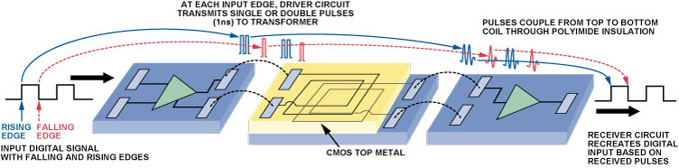
iCoupler technology (Figure 2) is a transformer-based approach to isolation. Integrating microtransformers and electronic circuitry, it has all the advantages of optocoupler-, discrete-transformer-, and semiconductor technologies—but without the disadvantages of optocouplers and discrete transformers. Optocoupler limitations include excessive power consumption, large timing errors, data-rate limitations, and sensitivity to temperature. In iCoupler-based products, insulation to meet the requirements of safety agencies is achieved through the use of a 20-µm-thick polyimide insulation layer between the transformer coils. It is capable of achieving an isolation rating of greater than 5 kV rms. This technology uses patented refresh circuitry, which updates the output to correspond correctly to the input state when input-signal transitions are not present, thus avoiding the inherent inability of discrete transformers to achieve correct dc levels.
iCoupler technology provides benefits in five key areas:
- Integration (size/cost)
- Performance
- Power consumption
- Ease of use
- Reliability
Isolation of IGBTs Using iCoupler Technology
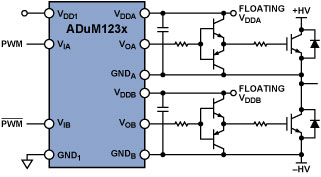
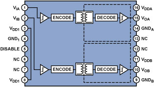
iCoupler technology can be found in a family of isolated gate drivers, including the 2-channel ADuM1233 (Figure 3), which offers isolation between the outputs and the inputs—and also between the two outputs—making it useful for isolating the controls of the IGBTs.
The input circuit’s power is provided by an isolated power supply and may require one or more stages of voltage conversion. A 5-V power supply is required for the microcontroller and the rest of the system, and the IGBT circuit requires 15 V for efficient operation. The iCoupler-isolated gate drivers must supply up to 100 mA of peak drive current, so an additional gain stage is required, as shown in Figure 4.
Because of the importance of the timing relationship between the two channels—with the IGBTs being driven by PWM signals in antiphase—the speed, stability, and reliability of the iCoupler technology are especially advantageous compared to LEDs and photodiodes. The curves in Figure 5 show that the propagation delays on the rising edges of the two channels are matched to about 100 ps—and on the falling edges to better than 1 ns—over the 12-V to 18-V output- and 4.5-V to 5.5-V input power-supply ranges.
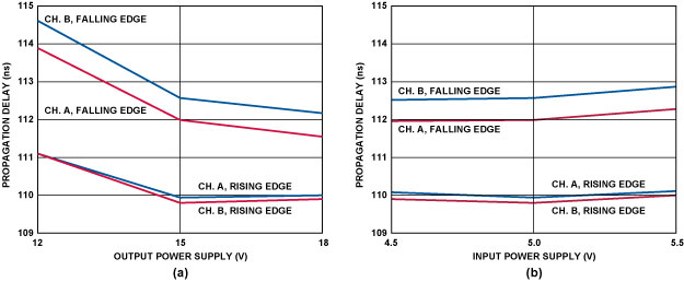
a) Output supply. (b) Input supply.
The resulting timing margins ensure fully complementary switching of the IGBTs, improving the efficiency of the power stage and the overall system.
As noted, the ADuM1233 offers true galvanic isolation between the input circuitry and the outputs of the device, and between the two output circuits. Each isolated output can operate at up to ±700 V with respect to the input, thus supporting the negative voltages of the low-side power supply (–HV in Figure 4). The difference between the high- and low-side supply rails (+HV and –HV) must not be greater than 700 V; however, this is compatible with the voltage rails typically used for powering inductive cooking.
Isolation of the User Interface with iCoupler Technology
If a capacitive keyboard is used, the interface between the microcontroller and the AD7147 or AD7148 capacitive keyboard controller can be implemented serially with either an SPI (serial peripheral interface, originated by Motorola) or I2C® (inter-integrated circuit, a Philips Semiconductor trademark). The bidirectional I2C interface is used for relatively low data-rate communication over short distances where low cost is important. I2C enables low cost by using only two bidirectional wires. This low-cost advantage is negated, however, when the I2C bus is isolated with optocouplers, which are unidirectional and cannot handle bidirectional signals. The transmit and receive signals from each wire must thus be separated, with the resulting four wires isolated with four optocouplers. In addition, a specialized buffer is required to eliminate lockup and glitches within the isolated interface. The extra components add cost and complexity, and they consume valuable board space.
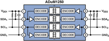
Integrated isolation solutions available in iCoupler technology reduce space requirements and design complexity at low cost. The ADuM1250 shown in Figure 6, and ADuM1251, embody true bidirectional isolation and incorporate a buffer to eliminate glitches and lockup. This degree of comprehensive integration limits the required external components to two bypass capacitors and two pairs of pull-up resistors (specified in the I2C standard)—and provides an I2C interface at low cost. Details on applying these devices can be found in AN-913 Application Note Isolating I2C Interfaces.
Pan Detection
It is important to detect the presence of the pan on the inductive hob. The IGBTs have to manage high voltage rails that are connected to their collector (+HV). By sampling these voltages with resistive dividers, a signal representing them can be sent to the microcontroller to detect any variation of the voltage at the collector of the IGBT. If a user chooses a heating level and places a pan on the inductive hob, the resultant energy transfer and current spike will produce a voltage variation at the collector, and thus at the resistive-divider output. When the pan is removed from the inductive hob, the change will be in the opposite direction. Thus, by comparing the voltage variation with a fixed threshold, using a comparator from the ADCMP3xx family, for example, the pan’s presence on the inductive hob can be detected. If no pan is detected, an interrupt is sent to the microcontroller, which will adjust the PWM frequency until the IGBTs stop providing current to the inductive element. This provides extra safety in case the user forgets to switch off the inductive hob.
CONCLUSION
Inductive cooking technology offers one example of the many useful applications of Analog Devices iCoupler digital-isolation devices. Today, a whole range of iCoupler products is available for general digital isolation and specialized applications. Some examples are shown in the selection table. Further information and an overview of the iCoupler technology can be found at www.analog.com/iCoupler.
致谢
The author would like to thank Andrew Erskine (applications engineer), David Krakauer (marketing manager for iCoupler products), and Mark Cantrell (applications engineer for iCoupler products) for their great advice and help in proofreading.
 客服微信
客服微信 查ic网订阅号