

System clock optimization can be both challenging and rewarding. It may be relatively easy to design an analog-to-digital converter encode circuit with a respectable 350 femtoseconds (fs) of jitter, but is this adequate for today’s high speed requirements? For example, when testing an AD9446-100—a 16-bit, 100-MHz ADC—at Nyquist with a 100-MHz sample clock, 350 fs of jitter can degrade the signal-to-noise ratio (SNR) by about 3 dB. When the same devICe is tested at the 3rd Nyquist zone with a 105-MHz analog input, the degradation can be as much as 10 dB. To reduce the clock jitter to a more tolerable 100 fs or less, the designer needs to understand where the clock jitter is coming from, as well as how much jitter the ADC can tolerate. It can be quite discouraging to realize—too late—that the clock-circuit performance is jitter-limited, and that this problem could have been more easily prevented during the design phase.
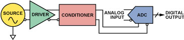
We will consider here the relevant clock specifications and means of achieving the expected performance of a high speed converter—employing a little know-how and experience. Starting with a typical ADC clocking scheme, such as that shown in Figure 1, we will highlight techniques that can be used to optimize the clock at each point in the signal chain—and identify some commonly used techniques that should be avoided.
What Is Jitter?
Jitter is probably the most important parameter in developing a good system clock circuit, so it is important to review some basics and understand what is meant by the term. Many technical papers describe the mathematics of jitter to the nth degree; however, design for good converter performance is not all about the exact description of jitter. One must also understand how it can get into the system and how to minimize its impact.
Jitter is variation in the placement of a clock edge; it will produce a timing error, leading directly to errors in conversion amplitude accuracy (Figure 2a). Increasing the analog input frequency increases the slope of the input signal, which magnifies the conversion error (Figure 2b). It is important to note that the magnitude of the conversion error is relative—a 0.5-LSB (least-significant-bit) conversion error for a 10-bit device is the equivalent of 32 LSBs of error for a 16-bit device. This means that jitter becomes more of a concern as both ADC resolution and analog input frequency increase.
Since this relationship is intuitively obvious, the engineer will ultimately determine how much jitter is acceptable by relating the ADC’s performance to the jitter of the encode clock. Equation 1 defines the SNR (dB)—with frequency—of a perfect ADC having infinite resolution, while Equation 2 is the SNR (dB) of a perfect ADC with N- (10, 12, 14, or 16) bit resolution.
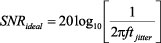 | (1) |
 | (2) |
Figure 3 combines these two equations. The intersections allow the user to determine the amount of total clock jitter that can be tolerated for a given analog input frequency. At low frequencies, the accuracy is limited by the resolution of the converter. As the input frequency increases, however, a point is reached beyond which the performance of the ADC is dominated by the total clock jitter of the system. For input frequencies to the left of the intersections, lower jitter is unlikely to be of concern.
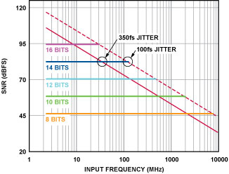
If the analog input frequency is near or to the right of an intersection, however, the frequency or resolution must be reduced—or the jitter specification must be improved. Thus, as the jitter intervals increase, the point where the SNR performance is dominated by the clock system jitter occurs at ever-lower frequencies.
For example, if a 14-bit ADC is tested using a clock that has 350 fs of jitter, the analog input frequency must be limited to frequencies below 35 MHz (the intersection of the 14-bit level and the 350 fs slope) to avoid significantly reduced performance. If the jitter can be reduced to 100 fs, input frequencies as high as 125 MHz can be handled.
In practice, this simplified model, using these first-order approximations, loses validity as the analog test frequency approaches the intersections. In order to fully understand the effect that clock jitter has on the ADC’s performance, the quantization noise and analog input amplitude need to be considered in addition to the resolution (Equation 3, based on Further Reading 9).
 | (3) |
where
SNR = Signal-to-noise ratio in dB.
fa = Analog input frequency of full-scale sine wave.
tj rms = Combined rms internal ADC jitter and external clock jitter.
ε = Average differential nonlinearity (DNL) of the ADC in LSBs.
N = ADC’s resolution in bits.
VNOISE rms = Effective input noise of ADC.
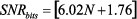
If tj rms = 0, ε = 0, and VNOISE rms = 0, the above equation reduces to the familiar
SNR = 6.02N + 1.76dB
For example, assume that an ADC has 0.5-LSB quantization noise and that, when tested, the analog input amplitude will be 0.5 dB below full scale. Figure 4, combining Equation 2 and Equation 3, shows that the encode clock jitter will affect the SNR performance at lower frequencies than in the simplified model.
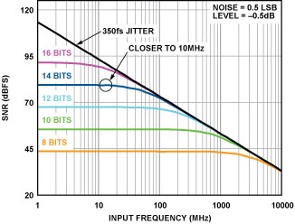
The earlier example showed that a clock with 350-fs jitter would not affect the SNR of a 14-bit ADC until analog input frequency approached 35 MHz. However, when the effects of quantization noise, input frequency, and input amplitude are considered, input frequencies as low as 10 MHz should be of concern. Likewise, 100 fs of jitter on the clock will also cause SNR degradation at frequencies lower than 100 MHz.
Keeping the Jitter Out
Now that the basics of jitter have been reviewed, we can consider sources of jitter. Anything that can modulate the edge transition of the ADC’s clock will introduce or affect jitter. These include crosstalk, EMI (electromagnetic interference), ground effects, and supply noise.
Crosstalk-induced jitter can occur in any two adjacent traces. If one trace carries a signal, and a nearby parallel trace carries a varying current, a voltage will be induced in the signal trace; if it is a clock signal, the time at which the clock edge occurs will be modulated.
Jitter can also be induced by EMI radiation on sensitive signal traces. EMI is produced by switching power supplies, high-voltage power lines, RF signals, and other similar sources. EMI produces similar effects to crosstalk by means of electrical or magnetic coupling that modulates the signal or clock timing.
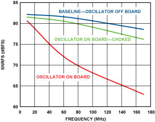
Figure 5 illustrates the effects of electromagnetic interference on SNR. The blue curve represents the baseline SNR-vs.-frequency of the AD9446, with an external clock and a linear power supply. The clock is not otherwise attached to the evaluation board in any way. The red curve shows the degradation that occurs when the same clock circuit is fixed or soldered onto the board, which is powered by a switching power supply. The green curve shows that substantial improvement in the converter’s performance can be obtained if the oscillator is choked and filtered off this supply.
Bouncing grounds due to switching currents or improper ground connections can also bring about jitter. Switching currents can become large when many gates are switching at the same time. This can induce current spikes on power and ground planes, level-shifting the threshold voltages on clock-circuit or analog-input signals. Consider the following example:
Assume a gate output has a 10-pF combined load from the PCB trace and input of the receiver gate. When the gate switches, 10 mA of dynamic current can flow into or out of each output. [10 mA is derived from 10 pF × 1 V/ns, the typical slew rate of a CMOS gate (I = C dV/dt).] A midscale transition could thus account for 120 mA of dynamic current if 12 gates are switching simultaneously. This would cause a large current spike to be drawn through the supply leads, one of which may be ground. The transient voltage drop (bounce) due to the lead resistance will affect all circuits that rely on it to be at ground potential.
To diminish the jitter caused by these sources, good layout practices and proper circuit partitioning should be employed It is essential to restrict analog circuits and digital circuits to their respective domains! This principle should be observed on every layer to ensure good isolation. It is important to understand how return currents flow relative to their source, and to avoid any encroachments or crossovers between analog and digital circuitry. In summary, sensitive analog inputs and clock traces must be kept away from other circuitry and traces that can influence them in undesired ways.
Improving Jitter Means Improving Slew
Now that the basics of jitter and its possible deleterious influences have been covered, one might ask, “How do I make improvements to my system clock or clock circuit so as to reduce jitter?”
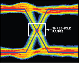
Recalling the initial discussion, jitter or noise can only corrupt the ADC’s timing when present during the transition or threshold period of the clock, shown in Figure 6. Making this edge (and hence the threshold period) faster by increasing the slew rate will inevitably lessen the amount of time that noise can be present during the threshold period and effectively lessen the amount of rms (root-mean-square) jitter introduced to the system.
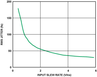
Keep in mind that increased slew rate doesn’t affect the original signal quality, only the transition time through the threshold region. To confirm this statement, refer to Figure 2b. Notice that with this faster signal swing less time is spent in the transition region. Figure 7 illustrates the inverse relationship between jitter and slew rate. Relating this to the earlier example, a 12-bit ADC requiring 100-fs minimum rms jitter for a 70-MHz analog input requires a slew rate of 1 V/ns.
Thus, minimizing jitter means improving the slew rate of the clock edge. One way this can be done is to improve the clock source itself. Figure 8 compares a number of different “off-the-shelf” oscillators when used as a clock source for one of ADI’s highest performing ADCs, the 16-bit, 80-MSPS AD9446, over a range of analog input frequencies.
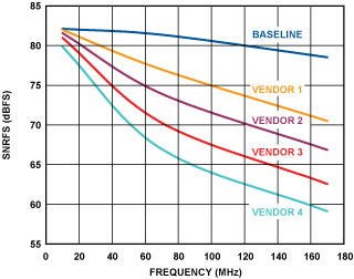
Typically, a custom high-performance clock oscillator is used to characterize the baseline performance achieved by Analog Devices ADCs (blue trace). Not all users of these high-speed converters can afford the cost or space required by a high-performance, oven-controlled, low-jitter oscillator, however, but available cost-effective oscillators can achieve reasonable performance, even at high analog input frequencies. Figure 8 shows the range of performance with some affordable devices.
An important point is that care should be taken when selecting an “off-the-shelf” oscillator, since oscillator vendors do not all tend to specify or measure jitter in the same way. A pragmatic way to determine which oscillator is best for the particular application is to collect a handful and test them in the system directly. By making this choice the only variable, a prediction of performance can be made (assuming that the oscillator vendor maintains reasonable standards of quality control). Better yet is to contact the oscillator manufacturer to obtain jitter- or phase-noise data, and get suggestions as to how to best terminate the device. Improper oscillator termination can seriously degrade the converter’s spurious-free dynamic range (SFDR).
Further Improvements
If the best oscillator available, based on price and performance, is still not adequate, one might consider using frequency division and/or filtering. Equation 4 describes the output of a sine-wave oscillator:
 | (4) |
Two parameters affect the slew rate—signal frequency (f) and amplitude (A). Increasing either of these will increase the slew rate and reduce the system clock jitter to a more desirable number. It is generally easier to increase the clock frequency. Frequency division will then be used to produce the desired converter clock rate, as well as to feed the other stages in the system clock tree.
Frequency dividers do add cost in terms of circuit components and power requirements. They also add jitter. Each active component added to the clock signal chain will increase the total jitter.
 | (5) |
When using a divider, all the relevant specifications must be considered. Typical among ADI’s clock-divider products is the AD951x family, which typically add only about 250 fs. In addition to having the dividing function built right in, features such as clock distribution and duty-cycle control are also available.
It is worth noting that clock dividers must contribute, however minimally, to the overall jitter on an absolute basis; but because of the frequency reduction they provide, their output jitter becomes a smaller fraction of the output period, and thus introduces less error. For example, if a 100-MHz clock source and other members of the chain contribute 800 fs of jitter (about 12.5% of the 10-ns period), and a clock divider reduces the frequency to 10 MHz, while introducing 250 fs of jitter, the resulting 840 fs of jitter is less than 1% of the 100-ns output period.
As a consequence of Equation 5, since the largest contributor dominates the overall jitter, the maximum jitter of the clock source should be no more than one-third of the largest contributor, but not necessarily a great deal less. The actual choices depend on the application’s performance requirements—such as for SNR over a given frequency range—the characteristics of available system components, and the usual limitations of size and cost.
Reducing Phase Noise
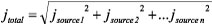
As Equation 5 indicates, total jitter is the root-sum-square (RSS) of the jitter from the clock cleanup circuitry, as well as the jitter in the source and any other intervening components. Thus, if the divider circuit is driven by an extremely noisy source, the full potential of the divider circuit may not be fully realized, simply because the largest jitter term dominates the equation. In this situation, consider using a passive, narrow-band filter between the clock source and the divider circuit.
To illustrate the advantages of filtering, consider a source having a jitter specification of 800 fs. If a clock divider circuit is placed between the source and the converter, the jitter can be reduced to roughly 500 fs even though the divider circuit is capable of much better performance. However, by placing a 5% LC band-pass filter between the source and divider circuit the jitter can be reduced to 250 fs. (See Figure 9).
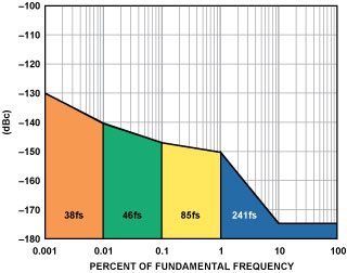
In order to understand how a filter can improve the jitter of a sinusoidal source, it can be useful to think of jitter in the frequency domain and estimate its value from a phase-noise plot. Although the calculation is straightforward and provides a good method of comparison, it doesn’t take into account nonlinear factors such as slew rate. As a result, this model will often predict more jitter than is actually present.
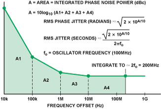
To perform the calculation, the phase-noise plot is divided into frequency regions, and the integrated noise power of each region is calculated, as shown in Figure 10. This permits identification of the jitter contribution from each region, as well as the total jitter of the source (by RSS summation). For these equations, f0 is the carrier frequency. The integrated phase noise is multiplied by the square root of 2 because the plot represents one of the two sidebands.
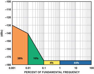
Consider now a source with 800-fs jitter. Plotting the phase noise of the source (Figure 11) makes it easy to determine where in the frequency domain most of the jitter is coming from. In the case of the clock with 800-fs jitter, it can be seen that the dominant part of the jitter in the spectrum is wideband. Therefore, emphasis in reducing wideband noise is paramount in sampled-type systems.
The use of a simple band-pass LC multipole filter with a 5% pass band (5% LCBP) on the output of the clock source can greatly improve the performance, as shown in Figure 11b. Note the improvement from 800 fs to less than 300 fs. That corresponds to an SNR improvement of over 12 dB.
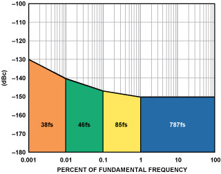
Five-percent LCBP filters can be easily obtained, but they can be big and expensive. An alternative is to use a crystal-type filter. Figure 12 shows the improvement in phase noise from 800 fs to less than 100 fs. This represents an additional 3-dB improvement over the 5% LCBP filter’s 12 dB, for a total of 15 dB!
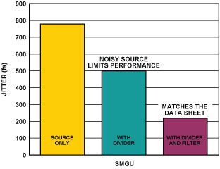
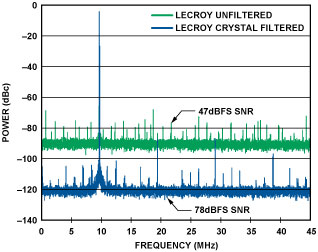
To demonstrate the effectiveness of cascading crystal filters with a noisy source, an experiment was performed using an old benchtop pulse generator to clock the 16-bit, 100-MHz AD9446-100 ADC. Unfiltered, the generator exhibited greater than 4 ps of jitter, resulting in an SNR degradation of over 30 dB. With the crystal filter applied the calculated jitter was close to 50 fs, providing an improvement in SNR approaching data-sheet typical performance (Figure 13).
Crystal filters, with their very narrow pass-band region—usually <1%—can reduce jitter from many sources to less than 100 fs, but they add expense and are bulkier than active filters. It is also worth noting that crystal filters have a limited input/output range of 5 dBm to 10 dBm. Pushing them beyond their specified range will result in distortion, possibly degrading the ADC’s SFDR. Finally, some crystal filters may require external components for impedance matching. Filters can do the job, but they require additional parts, tricky matching, and extra cost.
A quick summary of divider and filter solutions to improve the slew rate is shown in Table 1.
Table 1. Summary of Divider and Filter Trade-Offs
| Divider | 5% LCBP Filter | Crystal Filter | |
| Pros |
|
|
|
| Cons |
|
|
|
| Don’t Forget |
|
|
|
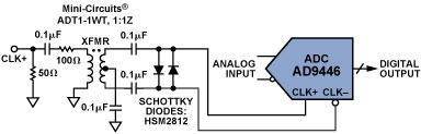
It is desirable to clip the signal before it approaches the ADC clock inputs using back-to-back Schottky diodes. This allows the source amplitude to be increased, thus increasing the slew rate, yet keeping the clock’s amplitude at a level compatible with the converter’s clock inputs.
If the clocking system is small or the last stage has short trace lengths, consider using a transformer in concert with the clipping diode. The transformer is passive and won’t add jitter to the overall clock signal. Transformers can also be used to provide gain for the oscillator’s signal voltage, increasing the A term (amplitude) in Equation 4. Lastly, transformers inherently provide pass-band filtering. Those with gain (1:2 or 1:4 impedance ratios) have narrower bandwidth, providing even better filtering of the clock signal. Transformers can also convert that single-ended signal into a differential signal—common and highly recommended in today’s ADC clock input interfaces.
Keep in mind that not all diodes will perform equally well (Figure 14). The “baseline” condition is the performance of the best-performing diode, relative to all the other diodes in this test batch, measured under the same conditions. Read the specifications carefully and pay particularly close attention to the dynamic resistance and total capacitance specifications. Diodes with low R and C values can improve clipping speed.
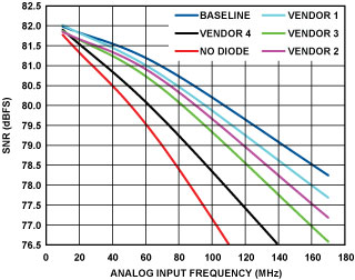
Here the AD9446, 16-bit, 80-MSPS ADC was used as a test platform; the only change was in the source of back-to-back diodes. The circuit used for this evaluation is shown in Figure 15.
Jitter Reduction in Clock Hardware Interfaces
There are many circuits and solutions that can be used when interfacing to the ADC’s clock input pins. However, a review of Equation 5
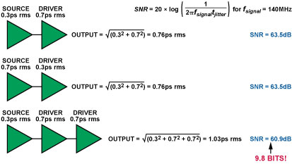
reminds us that a valid expectation is that each active component (oscillator source, driver or fanout gate, divider, etc.) in the signal chain will increase the total amount of jitter presented to the ADC’s clock input pins. Figure 16 shows that the addition of two gates, each contributing 700 fs of jitter, to a source with 300 fs of jitter can degrade resolution from about 12 bits to less than 10 bits at 140 MHz.
Thus, minimizing the number of components in the clock signal chain can help keep the total RSS jitter low.
The type of clock gates chosen is also worth noting. Simple logic gates are probably not the best choice when seeking to obtain good performance at high analog input frequencies. It is best to carefully read the data sheets of candidate devices and understand the pertinent specifications, such as jitter and skew. This is especially important when they are to work with sources that have extremely low jitter. For example, in Figure 17, Source A has 800 fs of jitter and Source B has 125 fs of jitter. With a crystal filter, the respective jitter levels can be reduced to 175 fs and 60 fs. However, a divider (or a gate with comparable jitter specifications) can increase the jitter to above 200 fs in both cases. This underscores the fact that proper selection and placement of clock drivers in the clock signal chain is important.

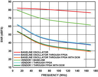
Another common approach leads to manifest inability to achieve data sheet performance. A flexible gate driver can be achieved fairly simply using an FPGA (often with a digital clock manager—DCM, which provides clock division). However, as Figure 18 shows, this approach has huge costs in degradation of SNR using the AD9446-80 (80-MSPS ADC); capable of achieving 13 bits ENOB, for example. The high-performance oscillator establishes the baseline SNR performance over a range of frequencies, as shown by the red curve. The green curve shows the difference in performance using the same clock, but with an FPGA as the gate driver between the high-performance oscillator and the converter. At 40 MHz, the FPGA reduces the SNR to 52 dB (8.7-bit performance) while the DCM contributes an additional 8-dB (1.3-bit) reduction of SNR. That performance difference is pretty alarming with 29-dB degradation in SNR, which means that the FPGA driver gate alone has an additive jitter of roughly 10 ps using Equation 1!
Choosing the best clock driver gate can be difficult. Table 2 gives a rough comparison of the additive jitter of a number of driver gates on the market. The suggestions on the lower half of the table may be helpful in attaining good ADC performance.
Table 2. Summary of Clock-Driver Gates and Their Additive Jitter
| Logic Family | Comments |
| FPGA | 33 ps to 50 ps (driver gates only, not including internal gates of DLL/PLL)1 |
| 74LS00 | 4.94 ps2 |
| 74HC700 | 2.2 ps2 |
| 74ACT00 | 0.99 ps2 |
| MC100EL16 PECL | 0.7 ps1 |
| AD951x Family | 0.22 ps1 |
| NBSG16, Reduced Swing ECL (0.1 V) | 0.2 ps1 |
| ADCLK9xx, ECL Clock Driver Family | 0.1 ps1 |
| 1Manufacturer’s specification. 2Calculated value based on degradation of ADC SNR. | |
CONCLUSION
It is critical to understand the entire clock system in order to achieve the best possible performance of the converter. Figure 3 and Equations 1 and 2 are helpful guides to clock requirements for applying either a jitter-limited ADC having very high resolution or a “perfect” N-bit ADC. If the analog input frequency is not well below the intersection of these lines, one must consider a clock source and associated circuitry with reduced jitter.
Decreasing the jitter of the system clock circuit can be achieved in many ways, including improving the clock source, filtering, and/or frequency-dividing, as well as proper choice of clock circuit hardware. Remember to pay attention to the slew rate of the clock. This will determine the amount of noise that can corrupt the converter during the transition time. Minimizing this transition time can improve the converter’s performance.
Use only necessary circuitry to drive and distribute the clock because each component in the signal chain will increase the overall jitter. Finally, don’t use “cheap” hardware gates; their performance is likely to be disappointing. One can’t expect championship performance from a $70,000 car outfitted with $20 tires.
| Divider | 5% LCBP Filter | Crystal Filter | |
| Pros |
|
|
|
| Cons |
|
|
|
| Don’t Forget |
|
|
|
| Divider | 5% LCBP Filter | Crystal Filter | |
| Pros |
|
|
|
| Cons |
|
|
|
| Don’t Forget |
|
|
|
| Divider | 5% LCBP Filter | Crystal Filter | |
| Pros |
|
|
|
| Cons |
|
|
|
| Don’t Forget |
|
|
|
| Divider | 5% LCBP Filter | Crystal Filter | |
| Pros |
|
|
|
| Cons |
|
|
|
| Don’t Forget |
|
参考电路
- AD6645 Data Sheet.
- AD9446 Data Sheet.
- Barrow, Jeff. “Reducing Ground Bounce in DC-to-DC Converters—Some Grounding Essentials.” Analog Dialogue, vol. 41, no. 2 (2007).
- Brannon, Brad. Application Note AN-756, “Sampled Systems and the Effects of Clock Phase Noise and Jitter.”
- Brannon, Brad and Allen Barlow. Application Note AN-501, “Aperture Uncertainty and ADC System Performance.”
- Curtin, Mike, and Paul O’Brien. “Phase-Locked Loops for High-Frequency Receivers and Transmitters—Part 2.” Analog Dialogue, vol. 33, no. 1 (1999).
- Custom Discrete Crystal Filters
• Filtronetics (www.filtro.net)
• Anatech Electronics, Inc. (www.anatechelectronics.com). - HSMS-2812 Data Sheet.
- Kester, Walt. Analog-Digital Conversion. Analog Devices (2004). Section 2.3, p. 2.72, Fig. 2.81.
- K&L Filter Data Sheets.
- Mercer, Doug, Steve Reine, and David Carr. Application Note AN-642, “Coupling a Single-Ended Clock Source to the Differential Clock Input of Third-Generation TxDAC and TxDAC+ Products.”
- Monolithic Crystal Filters (used for majority of evaluations)
• QuartzCom (www.quartzcom.com). - Smith, Paul. Application Note AN-741. “Little-Known Characteristics of Phase Noise.”
致谢
The authors would like to acknowledge and thank Yi Wang, Brad Brannon, and Walt Kester for their help and the benefits of their experience in this and related fields of study—and Ben Beasley for data collection in the laboratory.
 客服微信
客服微信 查ic网订阅号