

Built-in self-test (BIST), once reserved for complex digital chips, can now be found in many devICes with relatively small amounts of digital content. The move to finer line process geometries has enabled several Analog Devices data converters to include BIST functionality. For the chip manufacturer, BIST can help simplify the device characterization process by providing greater visibility into the device and can reduce manufacturing test time by allowing autonomous testing of some subset of the chip. Even larger benefits of BIST are realized at the system level when on-chip BIST functionality is incorporated into the system level design. As systems become more complex, integrating individual components with BIST, a hierarchical test strategy can be implemented, providing a powerful feature for enhancing system reliability.
At the system level, BIST functionality can be used in the design phase to characterize digital interface timing between the digital processors and the data converters. Without BIST, bit errors in the digital interface must be detected by changes in the converters’ noise floor. This type of error detection is much less sensitive than a digitally based BIST signature check, which can detect a single bit error. This same digital interface check can be performed on the production test floor, or in system level self tests in the field.
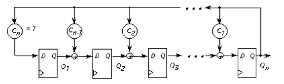
Figure 1 shows a basic BIST implementation. Incorporating BIST into a device requires the addition of three functional blocks: a pattern generator, a signature (or response) analyzer, and a test controller. The pattern generator stimulates the circuitry under test (CUT). The signature analyzer gathers the CUT’s response to the test pattern and compresses it to single value, referred to as a signature. The test controller coordinates the actions of the test circuitry and provides a simple external interface.
Pattern generators and signature analyzers are often implemented with linear feedback shift registers (LFSR). An LFSR with n flip-flops is shown in Figure 2. This type of pattern generator can produce pseudorandom patterns of width n, with 2n-1 unique combinations before repeating (every possible combination except all zeros). The pattern is completely deterministic when the initial conditions are known.
Signature analysis also makes use of LFSRs. Utilizing a second similarly constructed LFSR makes it possible to compress the CUT’s response to the entire pattern into a single value. This value is stored in a register at the completion of the test. The signature can then be compared with the expected signature to verify correct operation of the device. The process of compressing the response introduces the possibility of enabling a faulty CUT to produce a correct signature, but the probability of a fault going undetected becomes vanishingly small as the pattern length increases.
Using BIST at the System Level
At the board level, BIST functionality can aid in many types of testing. For example, testing the interface between a DAC and a digital data source can be accomplished by invoking the BIST signature analysis circuitry and using the digital source to provide the test pattern. In this case, the DAC manufacturer would provide the test pattern and the expected signature. The device has already been tested by the manufacturer, so an incorrect signature could be attributed to a faulty digital interface. Alternatively, the DAC manufacturer could provide an algorithm for generating the expected signature for an arbitrary test pattern. This provides greater flexibility in the patterns that the source can provide. Analog Devices provides BIST models, test patterns, and expected signatures for the AD9736 high-speed DAC.
The signature test is a pass/fail type of test. The specific value of an incorrect signature does not help diagnose the fault. However, the way the device is stimulated can provide some information about the type of fault. For example, different test patterns could isolate the fault to a specific input pin. When characterizing a digital interface, this type of test could be used to determine if there are any outlying connections that are responsible for reducing the timing margin of the overall bus. This information could be used to improve the board layout in a subsequent revision.
In some cases, the BIST pattern generator can be used in place of an external digital pattern generator, simplifying the evaluation of the device and the remainder of the downstream signal chain. The AD9789 contains an on-chip QAM mapper, interpolation filters, and a digital upconverter followed by a 14-bit DAC. The BIST pattern generator can be configured to send data to the QAM mapper. The device will transmit this data as a modulated signal. Analog performance can be measured at the output of the DAC and along the rest of the transmit path signal chain without any additional digital stimulus. This can expedite the evaluation of the analog portion of the design as it decouples the analog evaluation from the digital development and eliminates the special circuitry that would be required for digital test pattern generation.
Expect the inclusion of BIST circuitry on data converters and other “analog” devices to become increasingly common and more powerful as these devices move to smaller process geometries. As systems become more complex, inclusion of test capability is critical. As digital interface speeds increase, verifying that these interfaces are robust becomes more important and more difficult. Look for ways to use BIST functionality on individual devices to improve system level testability and device evaluation.


 客服微信
客服微信 查ic网订阅号