

BiometrICs and Security
The need for effective security, implemented efficiently, is manifest in today’s world. Individuals must be identified to allow or prohibit access to secure areas—or to enable them to use a computer, personal digital assistant (PDA), or mobile phone. Biometric signatures, or biometrics, are used to identify individuals by measuring certain unique physical and behavioral characteristics. Virtually all biometric techniques are implemented using a sensor, to acquire raw biometric data from an individual; feature extraction, to process the acquired data to develop a feature-set that represents the biometric trait; pattern matching, to compare the extracted feature-set against stored templates residing in a database; and decision-making, whereby a user’s claimed identity is authenticated or rejected.
Fingerprint Sensors
Fingerprints, long one of the most widely accepted biometric identifiers, are unique and permanent. Their images, formed of multiple curve segments, comprise high areas called ridges and low areas called valleys. Minutiae, the local discontinuities in the ridge flow pattern, are used as discriminating features. Fingerprint sensors “read” the finger surface and convert the analog reading into digital form through an analog-to-digital converter (ADC). Fingerprint sensors can be broadly classified as optical, ultrasound, or solid state—which includes capacitive, RF, thermal, and piezoelectric devices.
Because a finger’s outermost dry, dead skin cells have low electrical conductivity, an RF sensor acquires fingerprint data from the skin’s moist and electrically conductive boundary region where the live cells begin turning into keratinized skin. This live subsurface layer is the source of the fingerprint pattern, and it is rarely affected by damage or wear to the finger surface.
The AuthenTec® TruePrint® sensor uses a small RF signal between a conductive layer buried inside the silicon chip and the electrically conductive layer just below the surface of the skin. The RF field measures the electrical potential contours of the ridges and valleys of the finger’s underlying live epidermal layers. By acquiring data from the part of the skin that is untainted by injury or contamination, the sensor produces a more accurate and repeatable fingerprint sample than alternative optical or capacitive technologies that read only the surface of the skin.
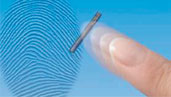
Pyroelectric materials generate a voltage based on temperature differentials. When a finger is in contact with a warmed sensor’s surface, the fingerprint ridges—which are closer to the sensor surface—retain a higher temperature than the valleys, which are farther from the sensor surface. The Atmel® AT77C104B FingerChip® sensor captures fingerprints using this type of thermal imaging. A linear sensor, it combines detection and data conversion circuitry in a single CMOS IC. Fingerprint images are captured by sweeping the finger over a sensing area. An image is produced when contact first occurs, but because it soon disappears as thermal equilibrium is reached, a sweeping method is necessary to acquire a stable fingerprint image.
The sensor, shown in Figure 1, captures the image of a fingerprint as the finger is swept vertically over the sensor window, as shown in Figure 2. The finger sweep technology ensures that the sensor surface stays clean. Unlike touch-based sensors, latent fingerprints do not remain once the finger has been removed. The sensor requires no external heat, light, or radio source. On-chip temperature stabilization identifies a temperature difference between the finger and the sensor, and increases the difference for higher image contrast. The discussion here will focus on a fingerprint recognition system based on this type of thermal sensor.
The main parameters that characterize fingerprint sensors include resolution, area, dynamic range, and number of pixels. Resolution is measured in dots (or pixels) per inch (dpi). Higher resolution allows better definition between ridges and valleys, and finer isolation of minutiae points—which play a primary role in fingerprint matching, since most algorithms rely on the coincidence of minutiae to determine if two fingerprint impressions are of the same finger. Larger sensing areas generally provide a more distinctive fingerprint, but sweeping the finger over a smaller sensor, and acquiring and processing the data rapidly, allows a small, low-cost sensor to achieve comparable definition to larger, more expensive sensors. Dynamic range, or depth, denotes the number of bits used to encode the intensity of each pixel. The number of pixels in the fingerprint image in a particular frame can be derived from the resolution and area.
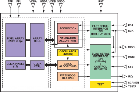
The AT77C104B sensor has 500-dpi resolution over a 0.4 mm × 11.6 mm area, providing a total of 8 pixels × 232 pixels, or 1856 pixels per frame. Each pixel is encoded with four bits, identifying 16 grayscale levels. Figure 3 shows a block diagram of the sensor, which includes the array, analog-to-digital converter, on-chip oscillator, control and status registers, navigation and click units, and separate interfaces for slow and fast modes of operation. Slow mode, which can run at up to 200 kHz, is used to program, control, and configure the sensor. Fast mode, which can run at up to 16 MHz, is used for data acquisition. An on-chip heater increases the temperature difference between the finger and the sensor. To limit current consumption, a watchdog timer stops heating the module after a specified length of time.
Modes of Operation
The sensor implements six modes of operation:
- Sleep mode: A very low-power-consumption mode, in which the internal clocks are disabled and the registers are initialized.
- Standby mode: A low-power-consumption mode, waiting for action from the host. The slow serial port interface (SSPI) and control blocks are activated; the oscillator remains active.
- Click mode: Waiting for a finger on the sensor. The SSPI and control blocks remain active; the local oscillator, click array, and click block are activated.
- Navigation mode: Calculating x- and y movements as the finger crosses the sensor. The SSPI and control blocks are still activated; the local oscillator, navigation array, and navigation block are also activated.
- Acquisition mode: Slices are sent to the host for fingerprint reconstruction and identification. The SSPI and control blocks are still activated; the fast serial port interface block (FSPI) and the acquisition array are activated. The local oscillator is activated when a watchdog timer is required.
- Test mode: This mode is reserved for factory testing.
Interfacing the Fingerprint Sensor to the Blackfin® Processor’s Serial Peripheral Interface
The Blackfin ADSP-BF533 low-cost, high-performance processor is chosen for this application because it combines the functions of a fast signal processor and a powerful microcontroller. Its 4-wire, full-duplex synchronous serial peripheral interface (SPI) has two data pins (MOSI and MISO), a device-select pin (/SPISS), and a gated clock pin (SCK). See Figure 4. The SPI supports master modes, slave modes, and multimaster environments. The SPI-compatible peripheral implementation also supports programmable baud rate and clock phase/polarities.
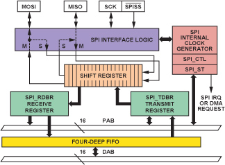
The interface is essentially a shift register that serially transmits and receives data bits—one bit at a time, at the SCK rate—to and from other SPI devices. The shift register enables the simultaneous transmission and reception of serial data. The SCK synchronizes the shifting and sampling of the data on the two serial data pins.
The SPI port can be configured as master (generates SCK and /SPISS signals) or slave (receives SCK and slave select signals externally). When the SPI port is configured as master, it drives data on the MOSI pin and receives data on the MISO pin. It drives the slave select signals for SPI slave devices and provides the serial bit clock (SCK). The Blackfin processor’s SPI supports four functional modes by using combinations provided by the clock polarity (CPOL) and clock phase (CPHA) bits. For detailed information on the Blackfin SPI port, refer to the ADSP-BF533 Blackfin Processor Hardware Reference Manual.
Hardware Interface
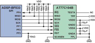
The seamless hardware interface between the ADSP-BF533 processor’s SPI port and the AT77C104B, shown in Figure 5, does not require any external glue logic. The slave select signals of the sensor, /SSS and /FSS, are driven through programmable flag pins PF1 and PF2. One flag should be configured as an output and driven high before the other flag is configured as an output (these flags should never be simultaneously configured as outputs, as the Blackfin processor, driving them low by default, would switch the sensor chip to scan test mode). Sensor interrupts, generated through the /IRQ pin, are read by input PF4. The reset, RST, is driven by PF3. Reset is an active-high signal, so a pull-down resistor is used on this line.
Application Software
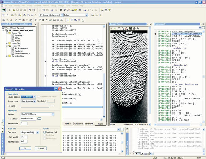
The application code performs tasks such as controlling the sensor, acquiring fingerprint data, and rearranging the data to display the received fingerprint image using the VisualDSP++® development tool’s Image Viewer plug-in.
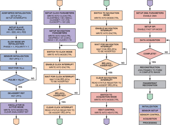
When the sensor detects a click (i.e., a signal indicating the presence of a finger), it generates an interrupt. The Blackfin processor receives this interrupt, and generates an interrupt on a falling edge. The STATUS register indicates the event that caused the interrupt. This process is used for navigation, read error, and other interrupts. A simplified flow chart of the complete application is shown in Figure 6.
Data Acquisition
Sensor heating is enabled in acquisition mode. The watchdog timer is also enabled, ensuring that heating remains controlled. Thus, when heating is requested, the sensor is heated for “n” seconds.
DMA parameters are then set up for data acquisition. Variable-size DMA flex descriptors are loaded into DMA parameter registers. The sequence of registers is essentially fixed, but the length of the descriptor is completely programmable. A 2D array is used to configure the DMA parameters. The 1D arrays are the individual descriptors. The first descriptor, a dummy, is used to receive the first five bytes because 40 dummy clock cycles must be sent by the sensor before the first data arrives in order to initialize the chip pipeline. Thus, the first synchronization sequences appear after 40 clock cycles. Data then arrives at every clock cycle for all following array readings.
The sensor sends data in the form of frames. The start of each frame is marked by the dummy column, which contains a synchronization word. The pixel array is read top to bottom, column by column, from the top left to the bottom right.
Data Rearrangement
The data must be rearranged to display the acquired fingerprint image. The rearranged data is stored and can be viewed using the VisualDSP++ Image Viewer utility. The acquired image and settings are shown in Figure 7. The following functions are performed:
- Nibble-swapping: The sensor sends data in a nibble-swapped format. A routine swaps the odd-even pixels for the entire frame.
- 4-bit to 8-bit conversion: Each sensor pixel is 4 bits wide, but the Image Viewer displays images with 8-pixel minimum width. Four bits of zero-padding converts each pixel to 8 bits.
- Level adjustment: Each pixel in the received data has an intensity of 0 to 15, but the display range is 0 to 255. Level translation of each pixel produces a good display.
- Array transpose: The data from the sensor is sent column-wise, but the 2-dimensional DMA receives data row-wise, so it must be transposed in order to display the frames continuously. A 3-dimensional array is used to get a continuous display of frames.
Fingerprint Reconstruction and Recognition
If the fingertip is swept across the sensor window at a reasonable rate, the overlap between successive frames enables an image of the entire fingerprint to be reconstructed using software supplied by Atmel. The reconstructed image is typically 25 mm × 14 mm, or 500 pixels × 280 pixels, with 8-bit resolution due to resolution enhancement. Each image thus requires 140 kB of storage. Larger or smaller images can be derived from this using standard image-processing techniques. once the frames have been joined to obtain a complete fingerprint image, recognition algorithms can match the sample with a template.
Trust but Verify
Fingerprint processing has three primary functions: enroll, search, and verify. Enrollment acquires a fingerprint image from the sensor and saves it in SRAM. The image is processed, enhanced, and compressed to create a fingerprint template. Various filters clean up the image and convert it to a mathematical representation, making it impossible to steal a template and directly recreate a fingerprint image.
Search compares a raw candidate image to a list of previously enrolled templates. Through a series of screening processes, the algorithm narrows the list of templates to a manageable size. Those templates that survive screening are compared to the candidate and verification scores are provided. A score exceeding a preset threshold indicates a positive identification.
Verification validates a user’s identity by comparing a raw candidate image to a previously enrolled template via real-time, closed-loop pattern-matching algorithms. A score is returned indicating the similarity of the candidate and template to generate a yes/no match decision.
Conclusion
The Blackfin processor and AT77C104B FingerChip sensor combine to provide simple, yet robust, fingerprint identification, enhancing security by allowing or prohibiting access to sensitive areas in buildings or sensitive data in laptop computers.
参考电路
- Blackfin Processors
- VisualDSP++
- ADSP-BF53x/ADSP-BF56x Blackfin Processor Hardware Programming Reference. Analog Devices. 2007.
- ADSP-BF531/ ADSP-BF532/ADSP-BF533 Blackfin Embedded Processor Data Sheet
- AT77C104B Data Sheet, “FingerChip Thermal Fingerprint Sweep Sensor.” Atmel Corporation.
- “AuthenTec Speeds Fingerprint Matching with Blackfin.” Blackfin Customer Case Studies. Dec 2004.
- Interfacing Atmel Fingerprint Sensor AT77C104B with Blackfin Processors. Engineer to Engineer Note EE-325. Aug 2007.
- Kreitzer, Kelvin and Alan Kasten. “New Fingerprint Subsystem Brings Biometrics to the Mass Market.” Embedded Computing Design. 2007.
- Maltoni, David, Dario Maio, Anil K. Jain, and Salil Prabhakar. Handbook of Fingerprint Recognition. Jun 2003.


 客服微信
客服微信 查ic网订阅号