

As mobile phone architectures have evolved, their power consumption and cost have decreased while their effICiency and performance have increased. Meanwhile, the wireless base stations that serve these phones have strived to keep up with these improvements. Over half of a modern base station’s power consumption is associated with the power amplifier, so continuous system-level efforts are being made to improve its energy efficiency. The time division multiple access (TDMA) architectures found in GSM, EDGE, and W-CDMA systems must be capable of ramping their power envelopes up and down within prescribed limits of power versus time. If critical ramp timing is not optimally managed, information can be lost on the transmit slot, or interference can be caused by transmission during the receive slot.
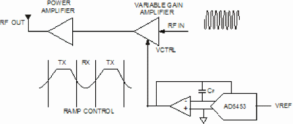
A high-speed current-output DAC can be used with a single op amp to generate a PA ramp profile that fits the RF gain requirements for TDMA. The ramp is applied to the voltage control pin of a variable-gain amplifier (VGA) to control the gain of the RF signal entering the PA, as shown in Figure 1. Specifying the offset, rise time, fall time, amplitude profile, and period information allows the DAC to curve fit the desired ramp. This profile information can be stored in the control logic of the microprocessor.
Ramp shapes, which vary for each modulation scheme, depend on the PA being used. Profiles can vary from simple ramped cosine type waveforms to more complex arbitrary waveforms. The advantage of using a current-output DAC coupled with a suitable high-speed op-amp is that it can precisely replicate both “slow” and “fast” ramp profiles. The key requirement for a DAC in ramp-control applications is fast settling time. Numerous voltage-output DACs will comfortably reach the specified accuracy, but current-output DACs combined with high-speed op-amps are still the best choice for settling times in the sub-100 ns range. The DAC will settle quickly as long as it is driven from a wideband low-impedance source such as a reference voltage. Consequently, the slew rate and settling time of a current-output DAC is predominantly determined by the op amp. Among the specifications that will determine the ac performance of the op-amp are its input capacitance—which must be kept to a minimum—and the small-signal bandwidth. Note that the DAC’s feedback resistor, on the order of 10 kΩ, is a significant load for the op amp to drive, and sets the dominant pole in determining the bandwidth of the circuit.
This leads to another advantage of choosing a combination of op amp and current-output DAC to generate ramp-control voltages: the op amp can be custom tailored to best fit the circuit design needs, where noise, settling time, and power requirements can all be taken into account. With the internal op amp found in voltage-output DACs, there is way to trade accuracy for bandwidth, but with an external op amp it is possible to find the optimal solution for the application. An op amp’s bandwidth typically has an inverse relationship to its dc precision. Two specifications that contribute to DAC accuracy are input bias current and input offset voltage. It is thus important to select an op amp with sufficient bandwidth to achieve the desired ramp performance, while still maintaining good dc precision. Choosing an op amp with excessive bandwidth will generally result in degraded dc performance.
An important component to take into account in achieving the desired settling time is the compensation capacitor. The DAC’s output capacitance introduces a pole into the open-loop response that can cause ringing or instability in the closed-loop ramp-profiling circuit. To compensate for this, an external feedback capacitor, CF, is connected in parallel with the DAC’s internal feedback resistor. Too small a value can produce ringing at the output, while too large a value can increase the settling time. The DAC’s output capacitance varies with code, so it is not possible to fix a precise value for CF.
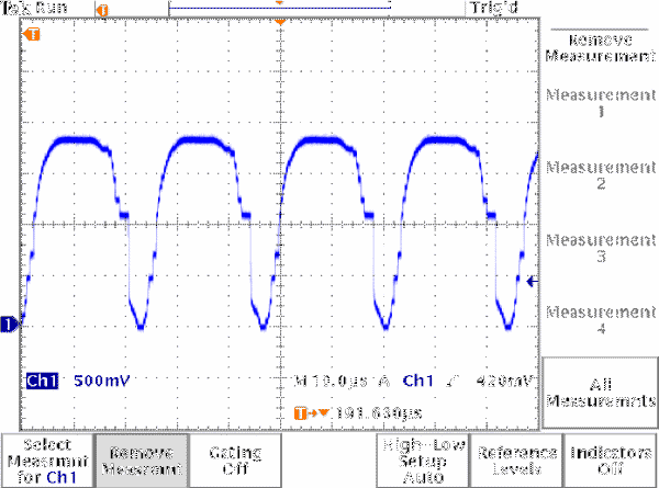
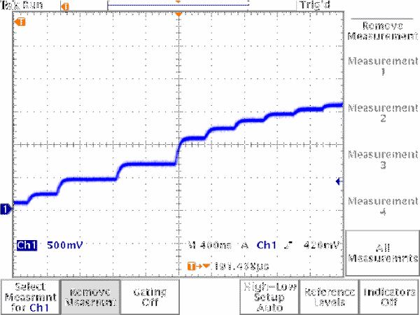
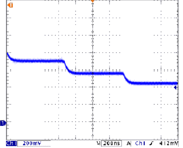
The AD5450/AD5451/AD5452/AD5453 family of DACs offers 8-/10-/12-/14-bit accurate current-output solutions for this application. Figure 1 shows an AD5453 DAC configured for a unipolar output, coupled with a high-speed buffer customized to best fit the performance of the system. With settling time on the order of 100 ns and a 12-MHz multiplying bandwidth, the part is ideal for waveform-generation applications. Figure 2 shows an example of a generic ramping profile. The magnified plots show that the DAC settles before the next data pattern is written to the SPI interface.


 客服微信
客服微信 查ic网订阅号