

Many of today’s high-speed op amps have on-chip input protection. In most cases, this protection is transparent to the user, but in some applICations it can be the circuit’s Achilles’ heel. This article discusses the need for input protection, its implementation, and its potential drawbacks. It also presents alternatives and circuit solutions that utilize amplifiers with input protection.
Various forms of input protection can be found in high-speed amplifiers: common-mode over-voltage protection, electrostatic discharge (ESD) protection, and input differential pair protection are some of the common ones. Common-mode over-voltage protection primarily limits the input voltage to be compatible with the safe operating range of the amplifier. ESD diodes protect the amplifier against static electricity, electrostatic induction, and other ESD events. These on-chip diodes are connected from the op amp inputs and outputs to the power supply rails. This protects the amplifier, as ESD currents are routed to the power supplies and bypass capacitors, rather than through the sensitive active circuitry.
Abrupt voltage changes across an op amp’s input can reverse bias the input differential pair, leading to latent defects, increased input bias current, and increased offset voltage. Protecting the differential input stage from damage is accomplished by limiting the voltage across the base-emitter junctions. In some higher-speed silicon processes, the base-emitter breakdown voltage (BVEBO) can be as small as 2 to 3 volts. Breakdown voltage is inversely proportional to process speed, so the faster a process is, the lower the breakdown voltage is. For reliable operation it is imperative to avoid reverse biasing the differential pair emitter-base junctions.
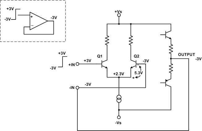
The amplifier is most susceptible to input stage damage when configured as a voltage follower. Real (non-ideal) amplifier outputs cannot respond instantaneously to a change at the input. The inability of the output to track the input means that the base-emitter junctions of the differential pair could be subjected to a potentially harmful reverse bias over-voltage condition. Figure 1 illustrates this principle. The input of the amplifier is connected to a pulse generator with a ±3-V output swing. For this discussion, it is assumed that the rise and fall times of the pulse generator are much shorter than the propagation delay of the amplifier. When the generator transitions from –3 V to +3 V, the amplifier input changes very quickly but the output does not, and a 5.3-V reverse bias develops across Q2. With transistors that have a rated BVEBO of 2 to 3 volts, input protection is clearly required.
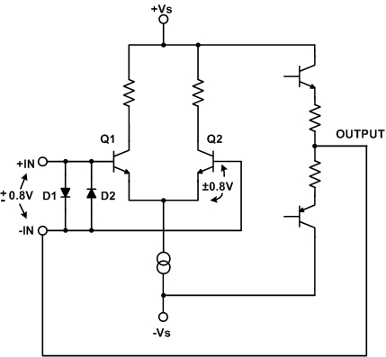
This protection can be as simple as a pair of back-to-back diodes (D1 and D2) across the amplifier inputs, as shown in Figure 2. With diodes D1 and D2 in place, the voltage swing across Q1 and Q2 is limited to about ±0.8V, well below the base-emitter breakdown voltage. The breakdown voltage is higher with slower speed processes, so more diodes can be added in series to increase the threshold voltage. If, for example, a process had a breakdown of 4 V, three series diodes could be used for a threshold of approximately 2.1 V. For very slow processes, the reverse breakdown voltages are high enough for input protection to be eliminated. Why not just leave a single set of diodes and be done with it? One of the drawbacks to input protection is that the diodes limit the voltage across the inputs, and therefore adversely affect slew rate. This is not a desirable feature when operating at high speeds.
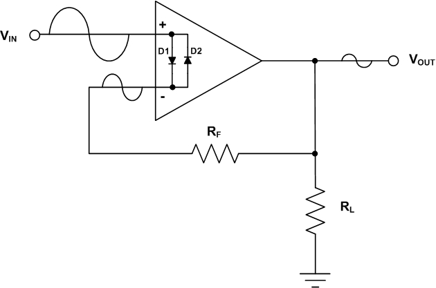
In most cases input protection does more good than harm. In rare situations, however, input protection can cause undesirable effects. Consider, for example, an amplifier that is not powered, but that has a signal at the input. Signal amplitudes of less than a few hundred millivolts will not present a problem, but signal amplitudes greater than about 400 mV can be problematic. With large input signals, input protection diodes (D1 and D2) will become forward biased. A signal path is established from the input to the output via the feedback resistor to the load, as shown in Figure 3. The amount of signal is dependant upon the amplitude and frequency of the input signal.
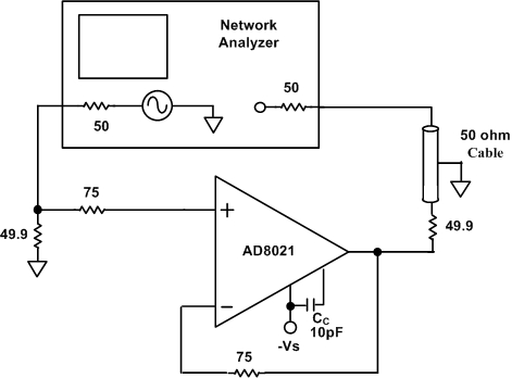
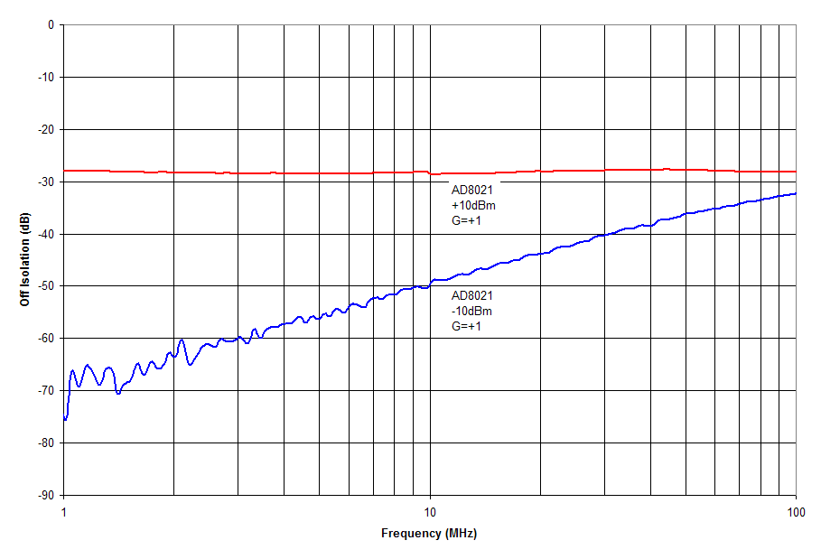
This principle is illustrated using an AD8021 configured for a gain of +1. As previously described, the AD8021 includes two on-chip back-to-back diodes across the amplifier inputs. The test circuit is shown in Figure 4. For this test, 200-mVpp (–10 dBm) and 2-Vpp (+10 dBm) signals were applied to the input. The signal was swept from 300 kHz to 100 MHz. Figure 5 shows the off isolation results. At 10 MHz, the 200-mV signal has an off isolation of approximately –50 dB. With the 2-Vpp signal, the protection diodes are fully turned on. A large portion of the input signal is fed to the output, and the off isolation is only –29 dB. This would have detrimental effects in multiplexed applications, such as radar detection, that require high levels of off isolation.
To solve this problem, first try to avoid it by selecting an amplifier with a higher differential voltage rating. Unfortunately, the amplifier has probably been chosen for numerous other parameters (differential input protection not being one of them). The absolute maximum ratings section of the amplifier’s data sheet usually shows its maximum differential input voltage. If the specification is less than ±Vs, some on-chip input protection is provided. The lower the voltage, the more likely the circuit could exhibit degradation in off isolation. Table 1 shows the differential input voltage ratings for selected amplifiers.
Table I. Maximum Differential Voltage Ratings of Selected High-Speed Op Amps
| Part Number | Max Differential Voltage (V) |
| AD8021 | ±0.8 |
| AD8007 | ±1 |
| ADA4899, AD8010, AD8036, AD8037 | ±1.2 |
| AD8027, AD8029, AD8099 | ±1.8 |
| AD8055, AD8014, AD8051 | ±2.5 |
| AD8023, AD8024 | ±3 |
| AD8031, AD8041 | ±3.4 |
| AD8005 | ±3.5 |
| AD8057, AD8038, AD8000 | ±4 |
| AD826 | ±6 |
| AD845, AD8061, AD8003, AD8045, ADA4860 | ±Vs |
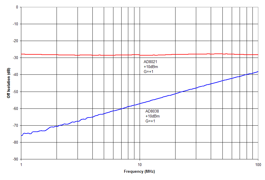
The off isolation test was repeated on the AD8038, a high-speed amplifier that has a differential voltage rating of ±4 V five times that of the AD8021. The larger input voltage rating means that it takes a larger signal to forward bias the input protection diodes. Figure 6 shows that the AD8038 provides off isolation of –57 dB at 10 MHz with a 2-Vpp signal at the amplifier input—a 28-dB improvement in off isolation as compared to the AD8021.
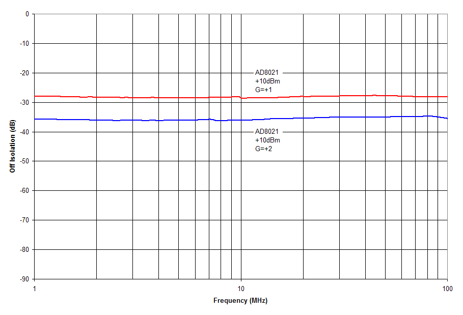
If the specified amplifier has a low differential input voltage rating, using it in a different configuration can help. Voltage followers have the highest amount of feed-through. A better option is to use the amplifier in a non-inverting configuration with gain. The feedback resistor forms a divider with the load, which provides attenuation of the feed-through signal at the output. Higher feedback resistances result in higher levels of attenuation. Don’t increase the feedback resistor too much, however, as this can increase noise and offset voltage, and, in some cases, it can also lower stability. Figure 7 compares the off isolation for the AD8021 configured for gains of +1 and +2 with 2-Vpp applied to the input. As shown, the gain-of-2 configuration provides a 6-dB improvement in off isolation as compared to the voltage follower configuration.
A more dramatic approach is to use a series analog switch, such as the ADG701, at the output of the amplifier. The ADG701 completely disconnects the output of the amplifier from the load, ensuring off isolation of approximately –55 dB at 10 MHz, an amount comparable to that provided by the AD8021 with a 200-mVpp input signal. Adding a switch is a good choice when a design requires an amplifier having key ac parameters, but not having a sufficient differential input voltage rating.
Amplifiers that include on-chip input protection provide problem free operation in most applications. On rare occasions, however, input protection may actually introduce problems. If this happens, first check the maximum differential input voltage specification. If low, consider using an amplifier with a higher rating, changing the circuit topology, or adding a series switch. All of these options will decrease the amount of feed-through and improve the off isolation.


 客服微信
客服微信 查ic网订阅号