

ADV3229相关信息来自ADI官网,具体参数以官网公布为准,ADV3229供应信息可在查IC网搜索相关供应商。
产品详情
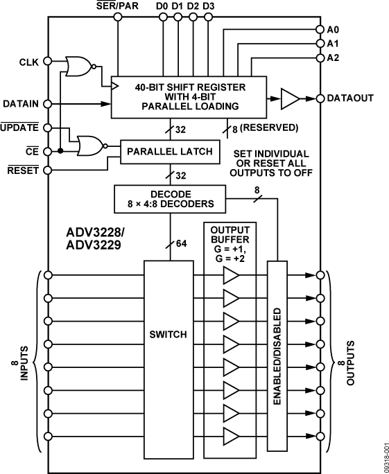
The ADV3228/ADV3229 are high speed 8 × 8 analog crosspoint switch matrICes. They offer a −3 dB large signal bandwidth of 750 MHz (ADV3228) and a slew rate of 2500 V/μs.The ADV3228/ADV3229 include eight independent output buffers that can be placed into a high impedance state for paralleling crosspoint outputs to prevent off channels from loading the output bus. The ADV3228 has a gain of +1, the ADV3229 has a gain of +2, and they both operate on voltage supplies of ±5 V. Channel switching is performed via a serial digital control that can accommodate daisy chaining of several devices or via a parallel control to allow updating of an individual output without reprogramming the entire array.
The ADV3228/ADV3229 are available in the 72-lead LFCSP package over the extended industrial temperature range of −40°C to +85°C.
Applications
- Routing of high speed signals including:
Video (NTSC, PAL, S, SECAM, YUV, RGB)
Compressed video (MPEG, wavelet)
3-level digital video (HDB3) - Data communications
- Telecommunications
优势和特点
- 8 × 8 high speed, non-blocking switch array
- Pinout and functionally equivalent to the AD8108/AD8109
- Drop-in compatible with ADV3224/ADV3225 16 x 8 array
- Complete solution
Buffered inputs
Programmable high impedance outputs
8 output amplifiers, G = +1 (ADV3228), G = +2 (ADV3229)
Drives 150 Ω loads - Operates on ±5 V supplies
- Low power: 0.5 W
- Excellent ac performance - Please see data sheet for additional information.
- Serial or parallel programming of switch array
- 72-lead LFCSP (10 mm × 10 mm)
ADV3229电路图
ADV3229中文PDF下载地址
ADV3229下载链接地址:https://www.analog.com/media/en/technical-documentation/data-sheets/ADV3228_3229.pdf

 客服微信
客服微信 查ic网订阅号